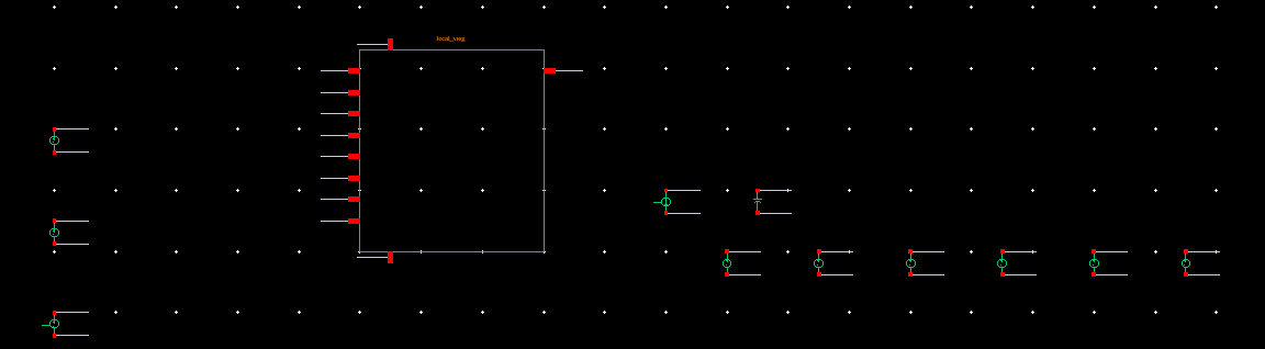
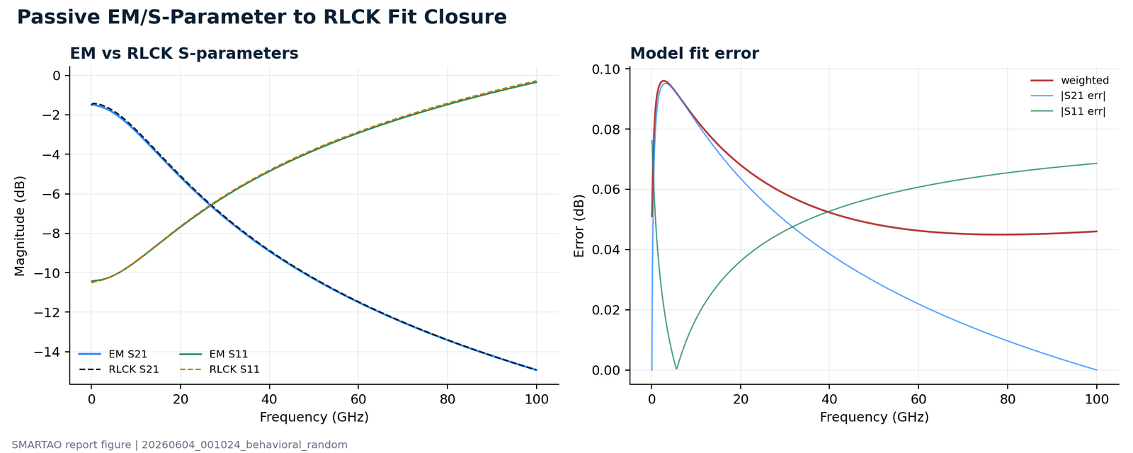
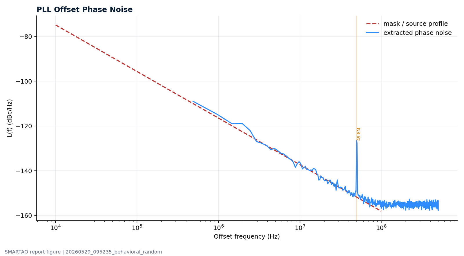
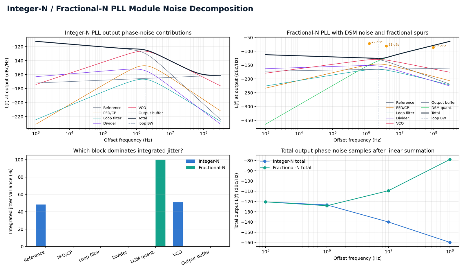
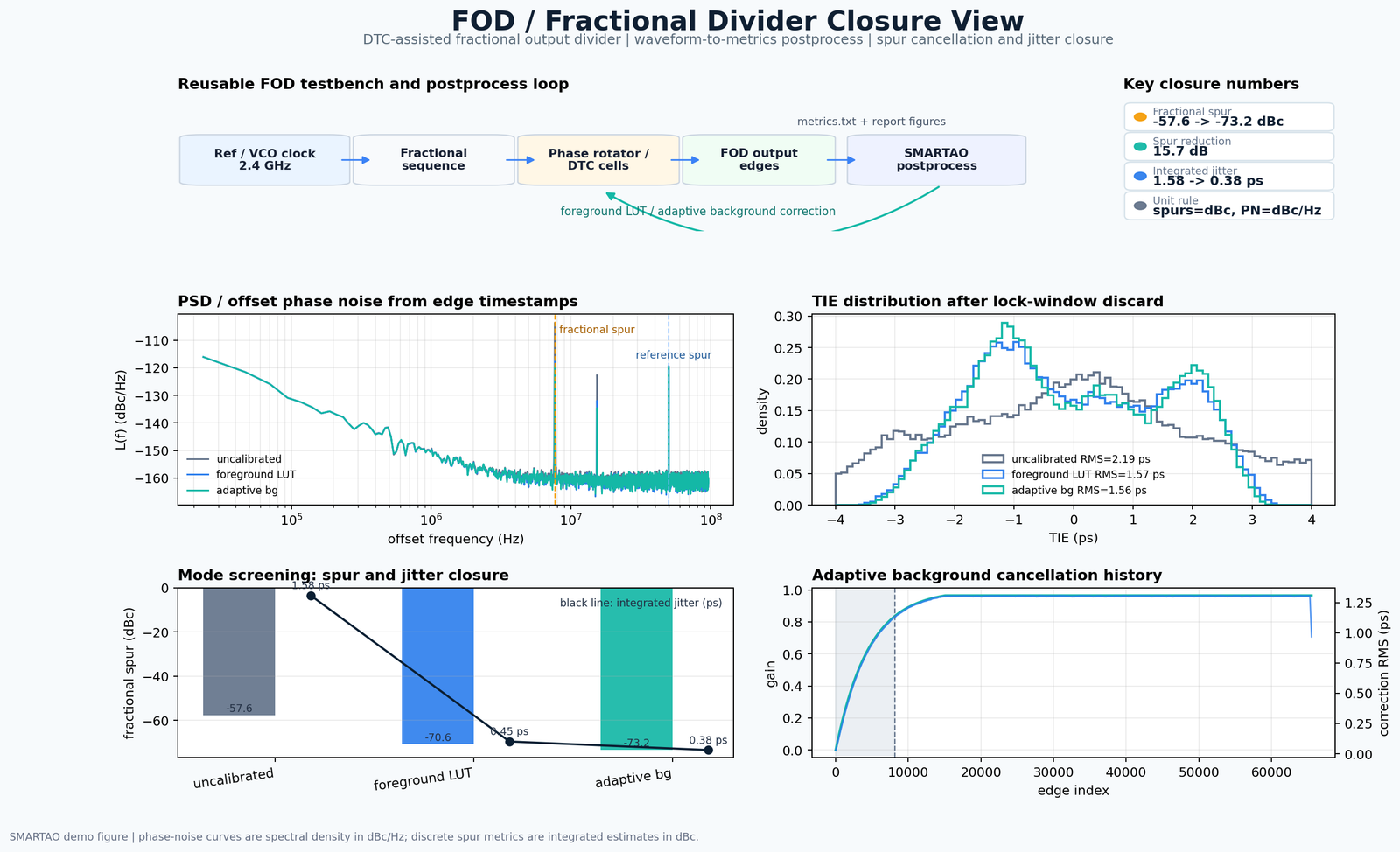
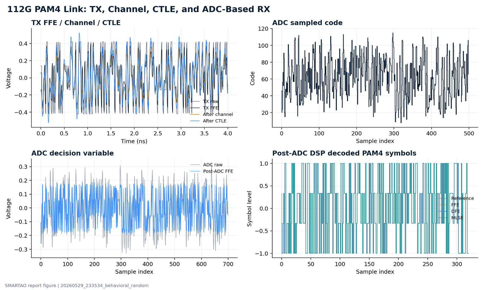
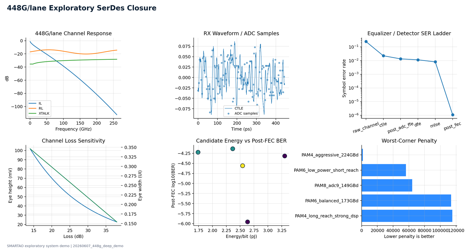
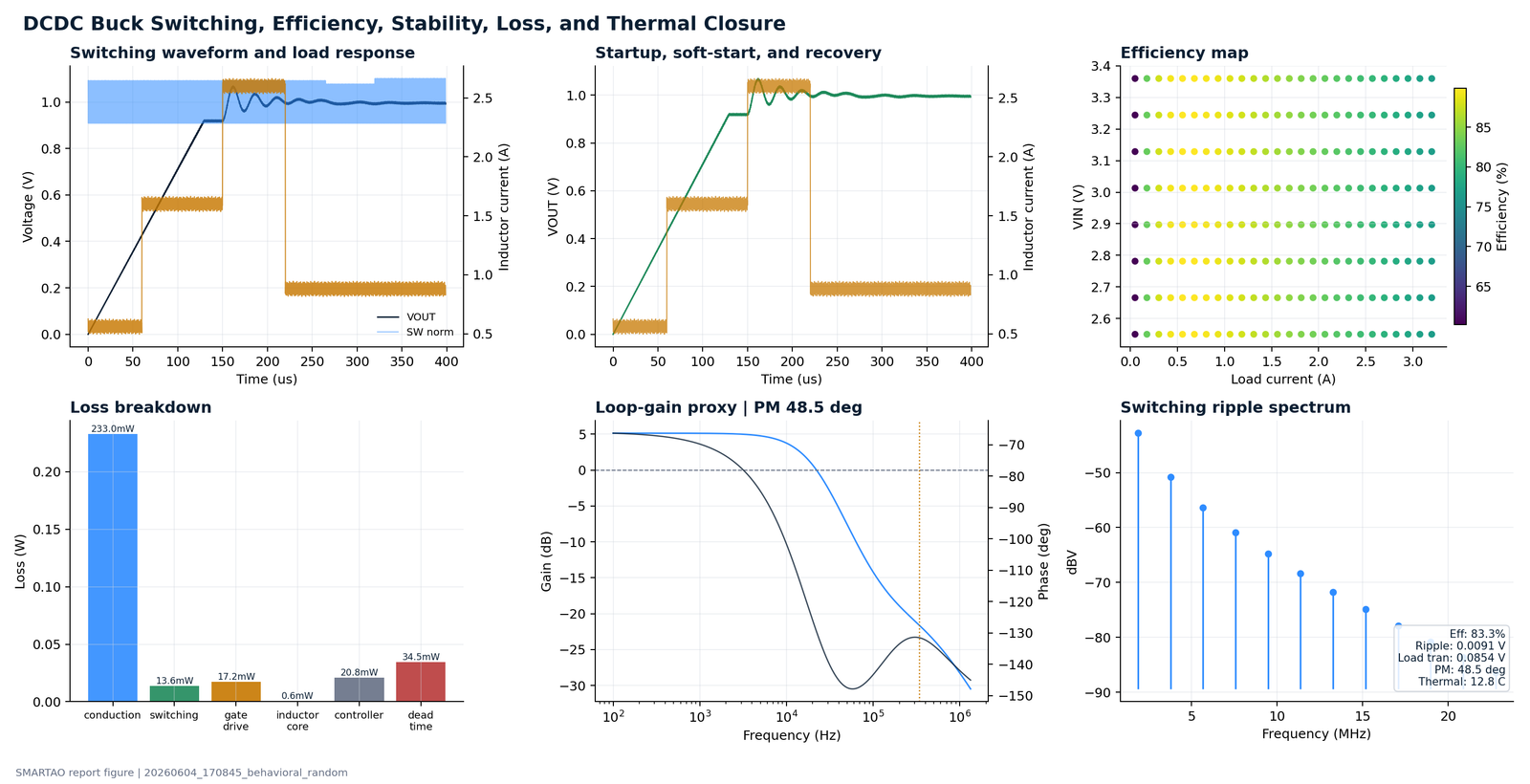
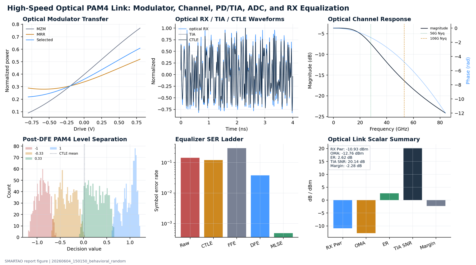
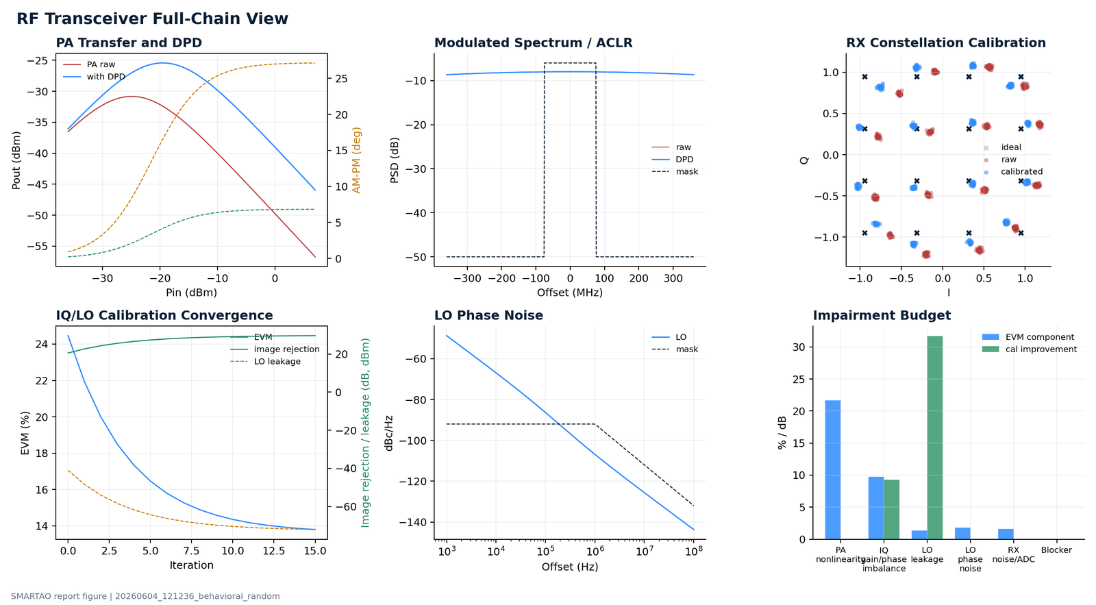
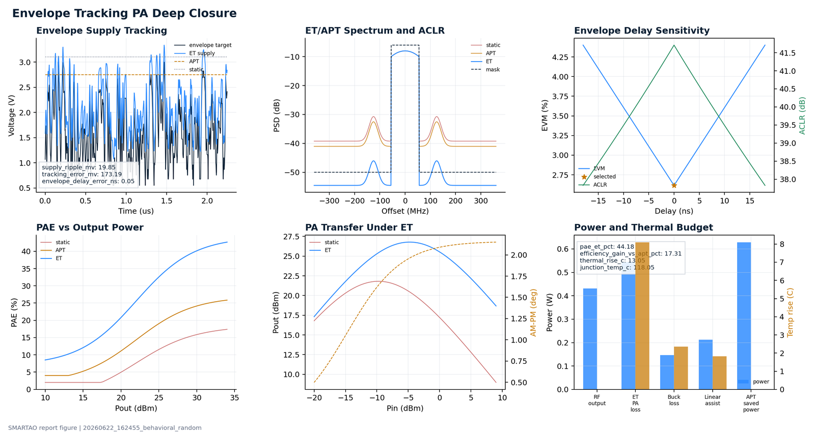
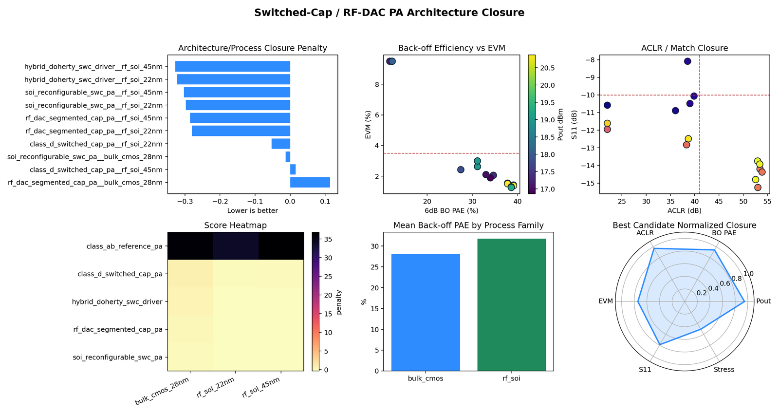
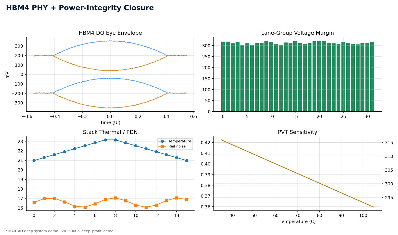
AI can assist the workflow while schematics, PDK data, layouts, and proprietary waveforms remain inside the company environment.
RF and analog teams can benefit from AI without exposing schematics, PDK data, or proprietary design details.
The key is to keep AI close to the workflow, but far from confidential implementation data. Instead of sending full schematics or layouts to an external model, teams can expose structured, limited information: block type, target specs, allowed variables, simulation status, metric names, and anonymized failure modes.
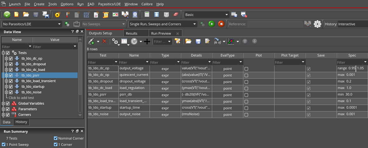
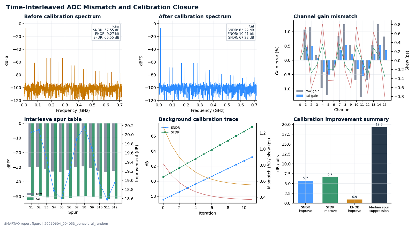
AI is especially useful around the design loop. It can help generate test plans, suggest likely measurements, organize optimization variables, explain failed simulations, compare candidate results, and draft reports. These tasks need engineering context, but not the full circuit.
A safe architecture separates three layers: a private layer for schematics, PDK files, simulation waveforms, extracted views, and customer-specific IP; a structured interface layer for sanitized specs, corners, variable ranges, metric outputs, logs, and workflow states; and an automation layer that applies approved actions locally.
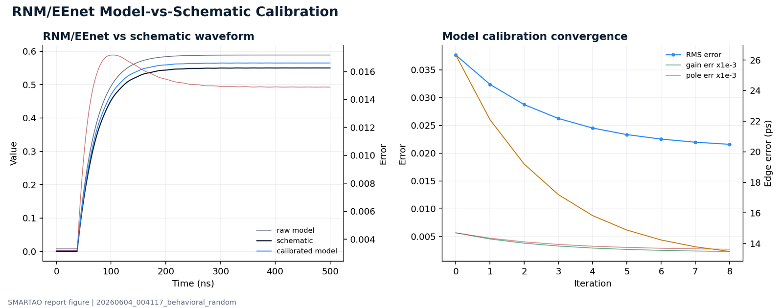
For RF/analog design, the most practical use of AI may not be generating a complete circuit. It may be helping engineers run better experiments, reuse knowledge, diagnose issues faster, and turn simulation data into decisions while keeping the real IP safely inside the design environment.