
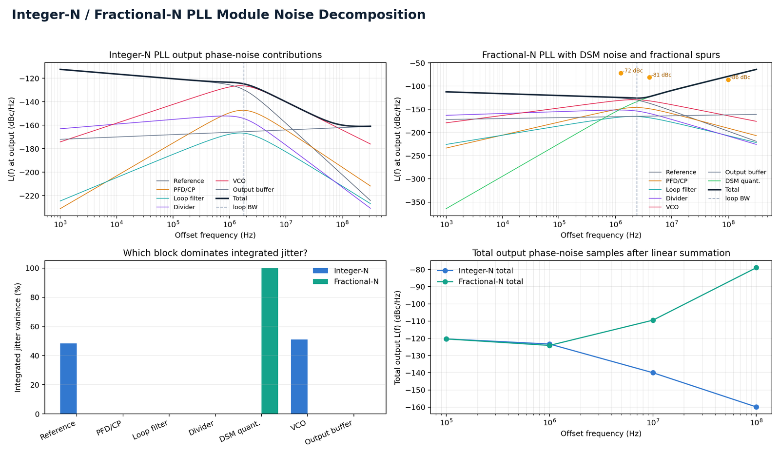
PLL module noise budget
Integer-N and Fractional-N output-referred noise from reference, PFD/CP, loop filter, divider, DSM, VCO, and output buffer summed into total L(f).
AnalogPilot turns reusable testbenches, Cadence-oriented simulation, metric extraction, optimization, behavioral/RNM modeling, system-level verification, and report generation into one practical engineering loop.
AnalogPilot is organized around reusable RF/analog module classes, end-to-end system scenarios, and customer-owned design instances. Developer-provided platform files and customer-generated workspaces are separated so upgrades do not overwrite private projects.
Module- and system-aware testbench packages include DUT wrapper contracts, variableized parameters, stimuli, node maps, OCEAN/MDL measurement hooks, and SKILL schematic-generation entry points.
Optimization reads normalized metrics.txt outputs, compares candidates, handles PVT/MC validation, and can write optimized variables back into Cadence-oriented collateral.
Behavioral, RNM/EEnet, and coarse/fine model flows support faster exploration, schematic equivalence checks, and reusable model calibration.
Registered preprocessors and postprocessors cover supply ripple, jittered clocks, PAM4, OFDM/modulation, fading/channel stress, ADC FFT, PLL phase noise, spurs, RF metrics, SerDes DSP, and system closure views.
A design intent can own multiple PDK-specific implementations. Each implementation is optimized and validated under its own PDK profile rather than pretending one schematic is portable.
Customers can add private design instances, architectures, and data locally. SMARTAO platform upgrades remain separate from customer-internal IP knowledge.
AnalogPilot is not just an IP module list. It provides repeatable flows for RF/mmWave, power management, data conversion, high-speed IO, clocking, passive/EM, sensors, automotive, wireless, radar, SATCOM, Bluetooth-style, memory-PHY, optical-link, and datacenter power-delivery system scenarios.
Reusable module classes, candidate architectures, and project-specific design instances are stored separately. A 1 V LDO, a 2 V LDO, and several LNA or SerDes front-end architectures can be optimized independently or compared in one candidate run without overwriting each other.
The homepage now highlights a small set of demos that tell the core story: prompt/spec intent can become verification-ready RF/analog, high-speed IO, photonic, packaging, power, and quantum-control workflows. The complete library remains available for deeper technical review.
Integer-N and Fractional-N output-referred noise from reference, PFD/CP, loop filter, divider, DSM, VCO, and output buffer summed into total L(f).
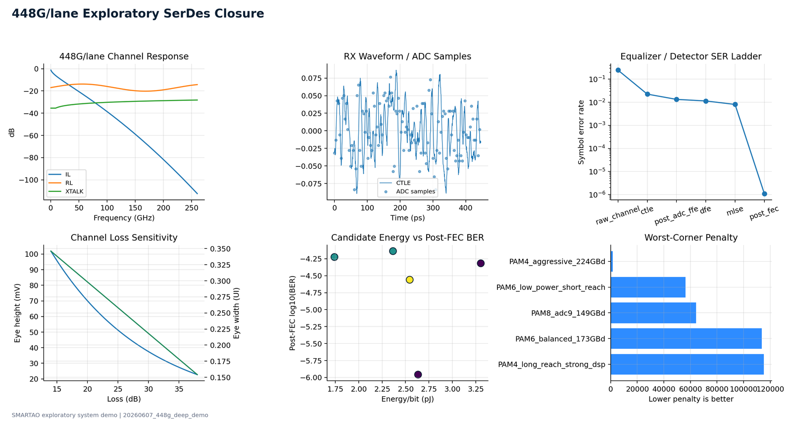
Forward-looking PAM4/PAM6/PAM8 architecture comparison with ADC-based RX, TX FFE, CTLE, FFE/DFE/MLSE, CDR, FEC waterfall, ADC-bit and channel-loss tradeoffs.
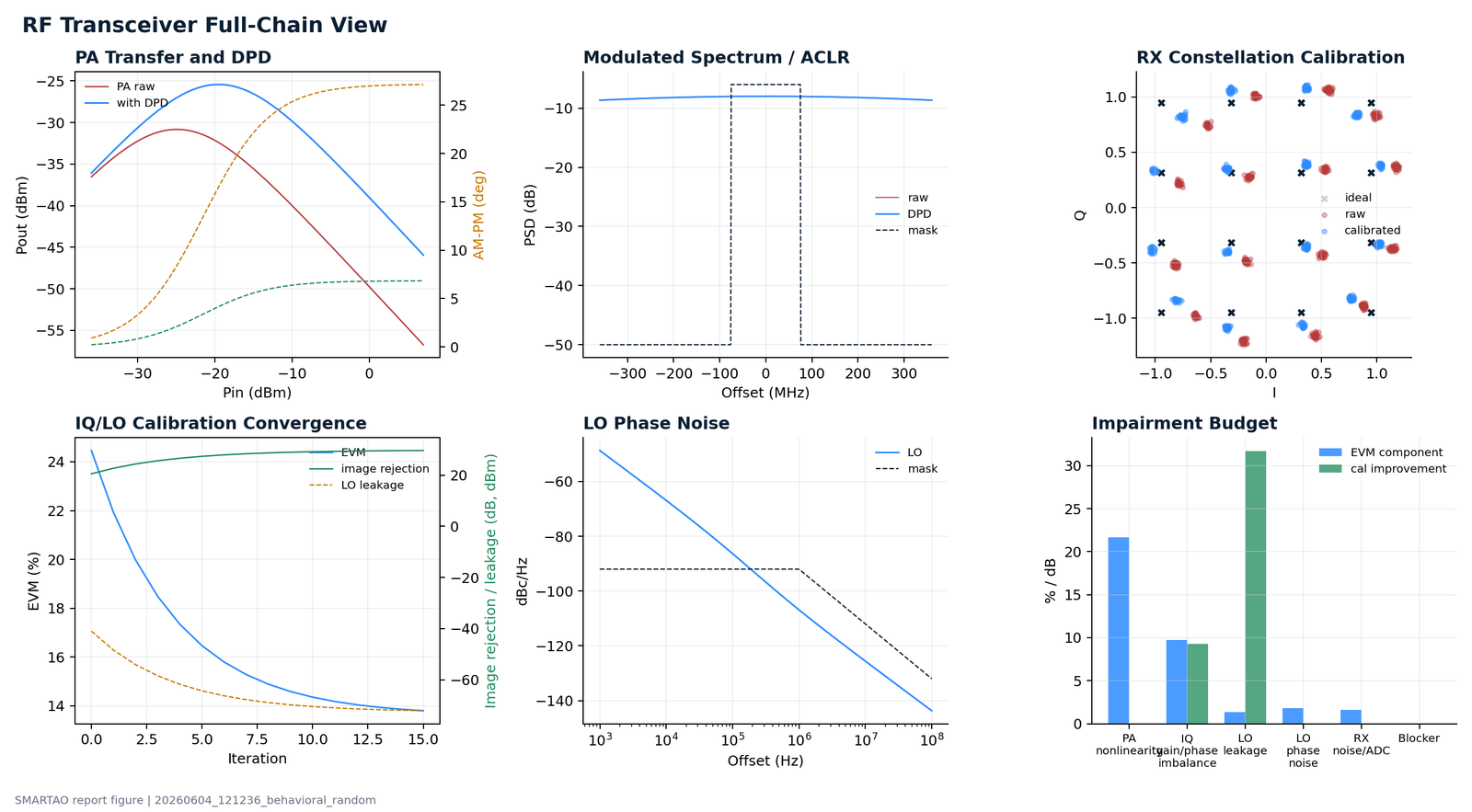
TX/RX impairment budget with DPD, PA nonlinearity, IQ imbalance, LO leakage, phase noise, EVM, ACLR, and calibration closure.
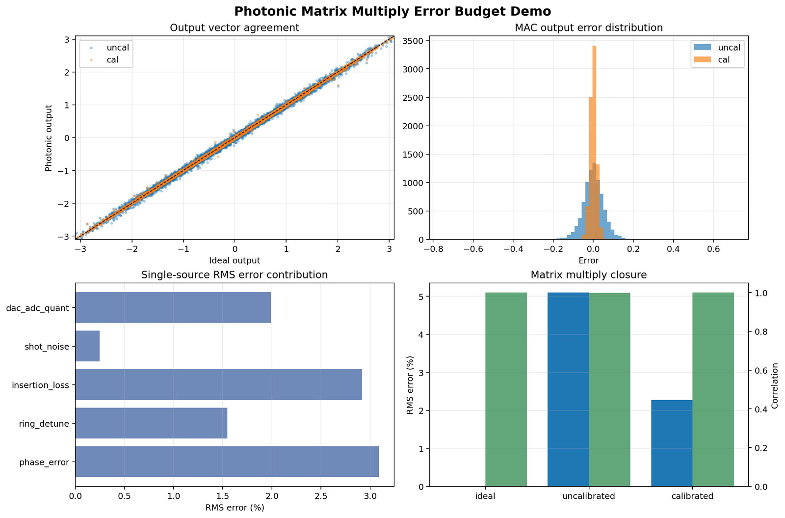
MZI/MRR weight bank error, optical loss, detector noise, thermal drift, calibration residual, and matrix-compute accuracy budget.
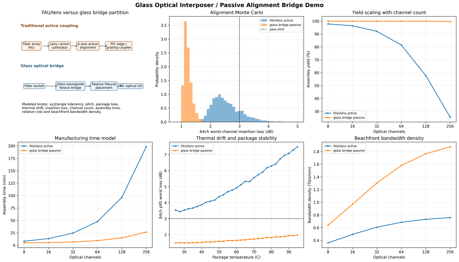
FAU/lens active coupling versus glass-waveguide bridge, insertion-loss Monte Carlo, yield, thermal drift, assembly time, and bandwidth density.
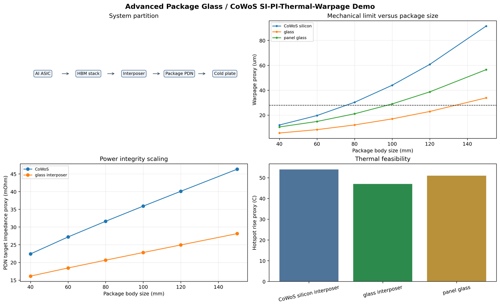
Chiplet interposer SI/PI, package thermal map, warpage, yield, cost index, and glass-versus-CoWoS tradeoff exploration.
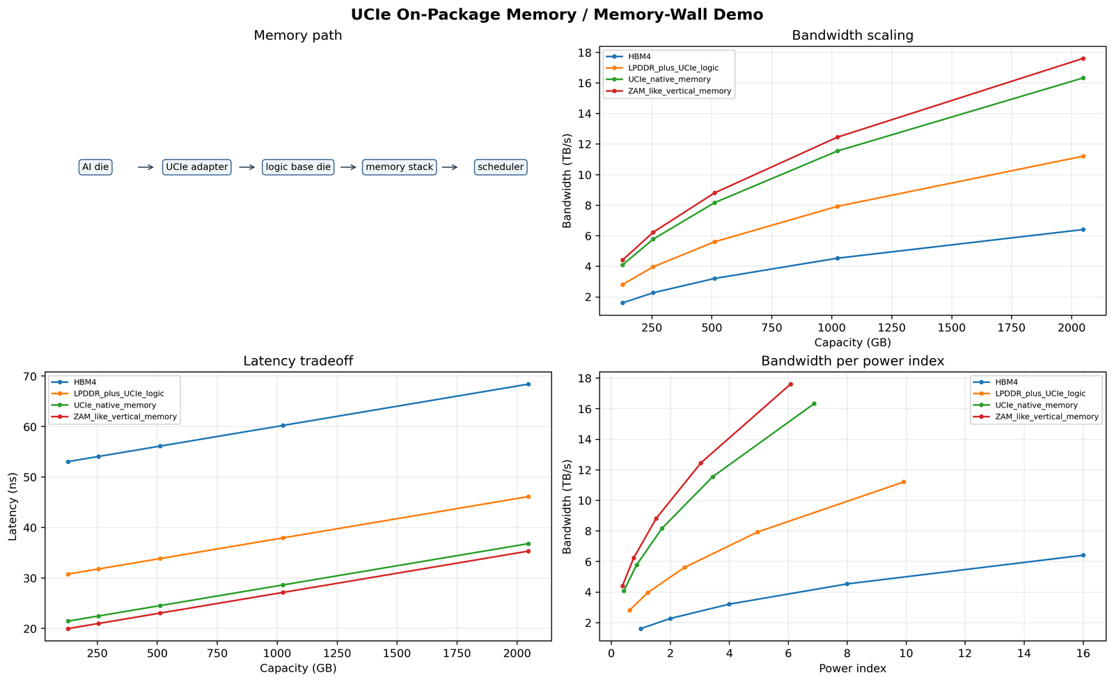
Compute-to-memory chiplet bandwidth, latency, package channel loss, energy-per-bit, thermal throttling, and throughput-per-watt tradeoff.
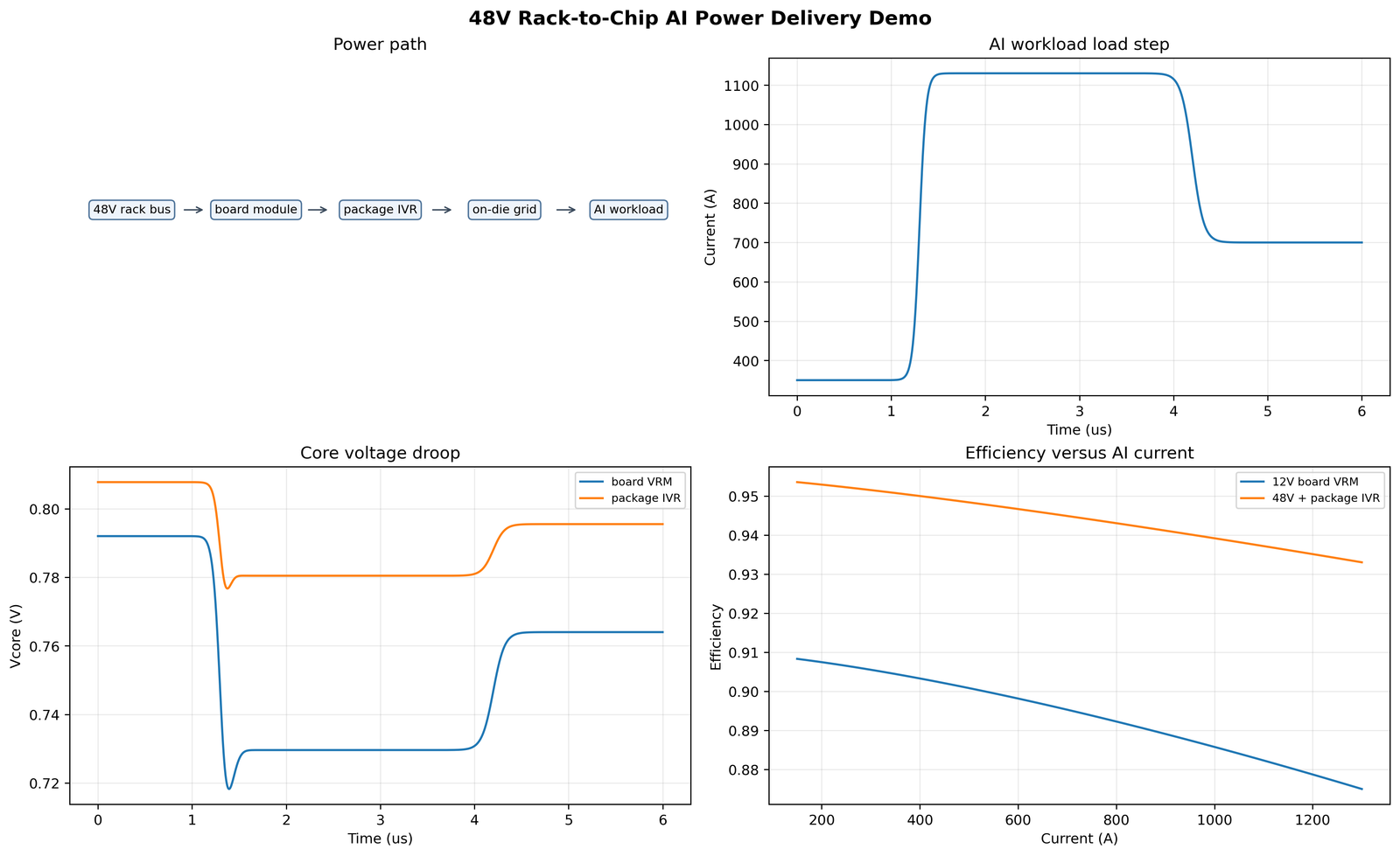
Rack bus, board converter, package IVR, on-die grid, workload load step, droop, efficiency, thermal rise, and energy-per-token closure.
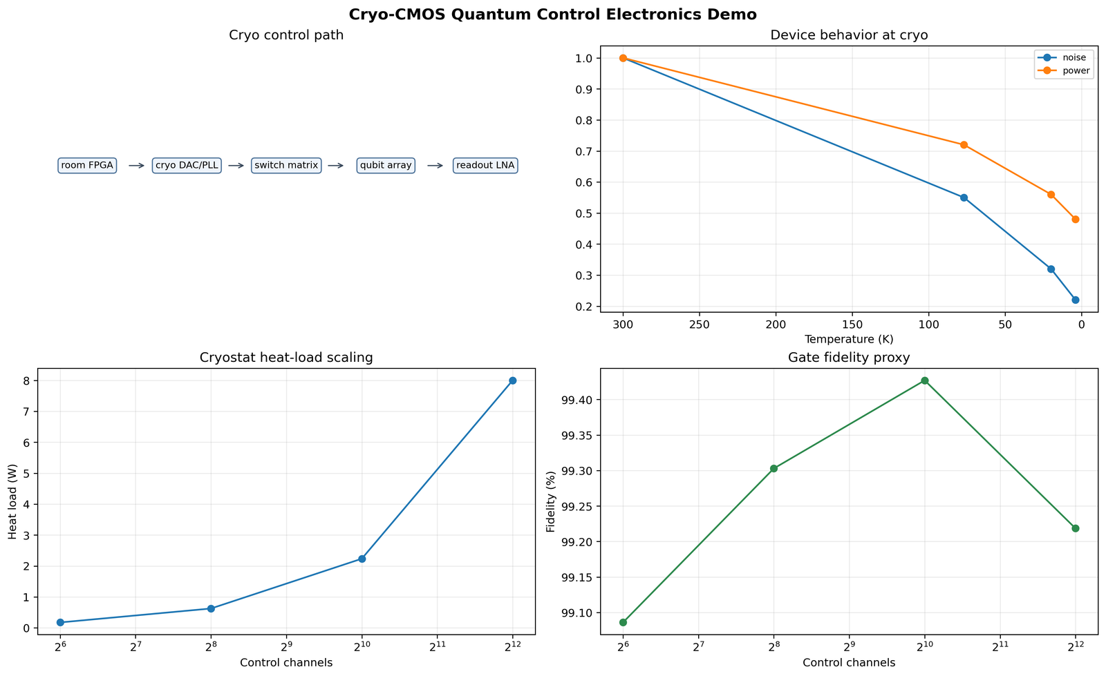
Cryogenic DAC/PLL/LNA chain, 4K heat load, drive phase noise, readout SNR, calibration time, and qubit-count scaling.
AnalogPilot is the long-term product. SMARTAO services help customers adopt it faster: connect the first real flow, integrate approved AI/LLM resources, and adapt verification, modeling, or reporting where a team needs a practical starting point.
Help a customer install and structure the workspace, connect Cadence/PDK profiles, port one real RF, SerDes, PLL, power, or system flow, and leave behind a reusable verification, optimization, and reporting template.
Connect customer-approved internal LLMs, private-cloud models, or external AI providers to AnalogPilot workflows with safe context boundaries, task routing, prompt templates, audit logs, and human approval points.
Adapt AnalogPilot for customer-specific post-processing, RNM or behavioral models, report formats, metric definitions, and internal design-review conventions while keeping the reusable platform flow intact.
LDOs, digital LDOs, DC-DC converters, battery paths, UVLO/POR, power integrity, automotive PMIC scenarios, and datacenter high-current PDN closure.
Integer/fractional PLLs, ADPLL/DCO, VCOs, FOD/phase-rotating dividers, DTC/TDC, LO distribution, jitter injection, phase-noise and spur workflows.
112G/224G/448G exploratory SerDes, ADC-based receivers, TX FFE, CTLE, FFE/DFE/CDR, MLSE/Viterbi post-processing, FEC waterfall views, and PAM4/PAM6/PAM8 stimulus generation.
LNA, PA, envelope-tracking PA, mixers, RF switches, phase shifters, front-end modules, mmWave phased arrays, radar, WiFi/cellular, and SATCOM-oriented tests.
SAR, sigma-delta, time-interleaved, pipelined, hybrid ADCs, DACs, sample-and-hold, code-density and FFT post-processing.
Inductors, transformers, baluns, transmission lines, couplers, filters, RLCK fitting, layout SKILL seeds, and EM-to-circuit closure.
AnalogPilot can start from an existing circuit block, system scenario, or internal demo and expand it into reusable simulation, system verification, optimization, modeling, and reporting infrastructure.
Define block/system goals, specs, corners, candidate architectures, and reusable variables.
Bind Cadence testbenches, node maps, stimuli, metrics, postprocess profiles, and report views.
Run optimization, PVT/MC validation, model calibration, visual reporting, and candidate comparison.
Reuse the verified flow across new design instances, architectures, PDK implementations, or related systems.
Project design data, PDK paths, simulation outputs, and local project knowledge can remain inside the deployment workspace. Platform files and project-specific instances are kept structurally separate.
SMART = intelligence, efficiency, automation. TAO = method, engineering path, tools, and discipline. The brand stands for practical automation that guides complex semiconductor design toward verifiable and reusable results.
These short technical notes explain the engineering principles behind reusable RF/analog automation: testbench infrastructure, high-speed link optimization, and AI-assisted workflows that respect design confidentiality.
Analog optimization is usually limited by how repeatable the measurement loop is, not by the optimizer itself.
Analog IP optimization is not limited by the optimizer. It is usually limited by how repeatable the measurement loop is.
For many analog and RF blocks, the real engineering effort sits in the testbench: biasing the DUT correctly, applying realistic stimuli, defining corners, extracting meaningful metrics, and making sure every candidate is evaluated in the same way. Without reusable testbench infrastructure, every optimization run becomes a fragile one-off experiment.
A good reusable testbench standardizes the interface between design variables, simulation setup, and measured results. The optimizer should not need to understand every schematic detail. It should see a clean parameter set and a consistent metrics file.
It also captures engineering judgment. The right load transient for an LDO, the right two-tone setup for an LNA, the right jitter and channel condition for a SerDes receiver, or the right FFT window for an ADC are all part of the design knowledge. Reusable testbenches preserve that knowledge.
Most importantly, reusable testbenches make results comparable. Architecture A, architecture B, different PDK corners, and later design revisions can all be evaluated through the same measurement contract. That is what turns optimization from trying many simulations into a disciplined design flow.
A single eye diagram can show whether one case looks open, but it cannot explain where the link margin came from.
An eye diagram is useful, but for 112G SerDes it is not enough.
At 112G PAM4, the link is a chain of tightly coupled impairments: TX FFE tap settings, package and channel loss, CTLE peaking, ADC resolution, clock jitter, CDR behavior, FFE/DFE adaptation, and sometimes MLSE or other sequence detection. A clean-looking eye at one point in the chain may not tell you why the link works, where the margin comes from, or what will fail across corners.
A stronger optimization flow needs stage-aware metrics. Before the receiver, we need channel insertion loss, return loss, crosstalk, and TX pre-emphasis. Inside the receiver, we need CTLE response, ADC input range, quantization noise, timing margin, and equalizer convergence. After detection, we need SER or BER estimates, error distribution, jitter tolerance, and adaptation stability.
It also needs realistic stimuli. PAM4 symbols, PRBS patterns, jitter injection, bandwidth-limited channels, and stressed channel conditions reveal problems that a simple waveform snapshot can hide.
A single eye diagram answers, does this case look open? A serious 112G SerDes optimization flow answers why it is open, how much margin exists, and which knobs actually created that margin.
AI can assist the workflow while schematics, PDK data, layouts, and proprietary waveforms remain inside the company environment.
RF and analog teams can benefit from AI without exposing schematics, PDK data, or proprietary design details.
The key is to keep AI close to the workflow, but far from confidential implementation data. Instead of sending full schematics or layouts to an external model, teams can expose structured, limited information: block type, target specs, allowed variables, simulation status, metric names, and anonymized failure modes.
AI is especially useful around the design loop. It can help generate test plans, suggest likely measurements, organize optimization variables, explain failed simulations, compare candidate results, and draft reports. These tasks need engineering context, but not the full circuit.
A safe architecture separates three layers: a private layer for schematics, PDK files, simulation waveforms, extracted views, and customer-specific IP; a structured interface layer for sanitized specs, corners, variable ranges, metric outputs, logs, and workflow states; and an automation layer that applies approved actions locally.
For RF/analog design, the most practical use of AI may not be generating a complete circuit. It may be helping engineers run better experiments, reuse knowledge, diagnose issues faster, and turn simulation data into decisions while keeping the real IP safely inside the design environment.
AnalogPilot is suitable for internal IP development, Cadence-centered circuit/system automation, reusable modeling infrastructure, and technical discussions around RF/analog IC and system-level automation.
A SMARTAO product
Founder: Yusheng (Boris) Chen
RF/Analog IC automation and mixed-signal systems
WeChat: Smartaoai
SMARTAO company site: www.smartao.ai
Download vCard · Open vCard QR

AI-powered · Engineer-driven · RF/Analog Innovation